


Electron spin states can now be probed at much higher resolution and more efficiently, opening new opportunities in materials analysis and data processing technologies.
Researchers Koichiro Yaji and Shunsuke Tsuda at the National Institute for Materials Science in Japan have developed an improved type of microscope that can visualize key aspects of electron spin states in materials. The quantum mechanical property of electrons called spin is more complex than the spin of objects in our everyday world but is related to it as a measure of an electron’s angular momentum. The spin states of electrons can have a significant impact on the electronic and magnetic behavior of the materials they are part of.
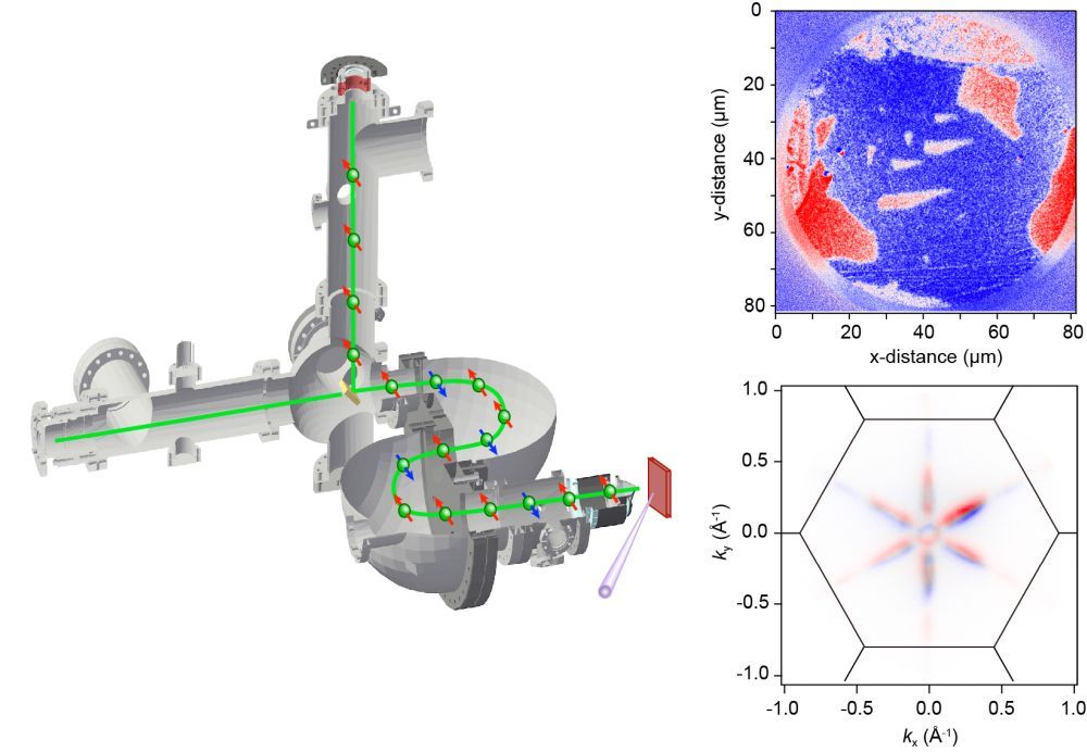
The technology developed by Yaji and Tsuda is known as imaging-type spin-resolved photoemission microscopy (iSPEM). It uses the interaction of light with the electrons in a material to detect the relative alignment of the electron spins. It is particularly focused on electron spin polarization – the extent to which electron spins are collectively aligned in a specific direction.
The team’s iSPEM machine consists of three interconnected ultra-high vacuum chambers for preparing and analyzing the sample. Electrons are emitted from the sample by absorbing light energy, accelerated through the apparatus, and then analyzed by interaction with a spin filter crystal. The results are displayed as images which experts can use to glean the necessary information about the electron spin states in the sample.
“Compared to conventional machines, our iSPEM machine drastically improves the data acquisition efficiency by ten-thousand times, with a more than ten-times improvement in spatial resolution, ” says Yaji. “This offers tremendous opportunities for characterizing the electronic structure of microscopic materials and devices at previously inaccessible levels in the sub-micrometer region.”
This advance could promote improvements in using electron spin states in information processing and other electronic devices, as part of the fast-developing field know as spintronics. In spintronics applications, the spin state of electrons is utilized to store and process information, in addition to the traditional use of electric charge.
“This could lead to more energy-efficient and faster electronic devices, including quantum computers” says Yaji. Applying the subtleties of quantum mechanical behavior to computing is at the forefront of efforts to take computing powers to another level, but until now most advances have been restricted to arcane demonstrations rather than practical applications. Mastering the understanding, control and visualization of electron spin could be a significant step forward.
“We now plan to use our machine to investigate the possibilities for developing a new generation of electron spin-based devices, because it will let us look into the properties of tiny and structurally complex samples previously hidden from view,” Yaji concludes.
Further information
Name: Koichiro Yaji
National Institute for Materials Science
Email: yaji.koichiro@nims.go.jp
Paper: https://doi.org/10.1080/27660400.2024.2328206
About Science and Technology of Advanced Materials: Methods (STAM-M)
STAM Methods is an open access sister journal of Science and Technology of Advanced Materials (STAM), and focuses on emergent methods and tools for improving and/or accelerating materials developments, such as methodology, apparatus, instrumentation, modeling, high-through put data collection, materials/process informatics, databases, and programming. https://www.tandfonline.com/STAM-M
Dr Yasufumi Nakamichi
STAM Publishing Director
Email: NAKAMICHI.Yasufumi@nims.go.jp
Press release distributed by Asia Research News for Science and Technology of Advanced Materials.